当前位置:网站首页>Detailed explanation of the principle of triode series linear voltage stabilizing circuit and Multisim Simulation
Detailed explanation of the principle of triode series linear voltage stabilizing circuit and Multisim Simulation
2022-07-20 09:52:00 【Continuous progress】
List of articles
Preface
During this period of time, I came into contact with Based on triode 、 Voltage regulator diode realizes voltage reduction and voltage stabilization Circuit . When you are familiar with circuits and reading articles , I found many articles about Triode linear voltage stabilizing circuit The principle of is not introduced in detail 、 An incorrect question .
This paper first introduces the design of triode Input / Output characteristic curve , And use on this basis Multisim Build a triode voltage stabilizing circuit , Finally, the voltage stabilizing circuit is Principle analysis .
One 、 Triode input / Output characteristic curve
1. Input characteristic curve
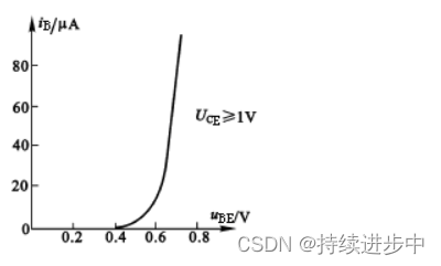
When the common emitter of the triode is connected , Voltage between collector and emitter U C E U_{CE} UCE When maintained at different voltages , reflect U B E U_{BE} UBE And i B i_B iB A series of curves of the relationship , Called triode Common emitter input characteristic curve .
In general , When U C E ≥ 1 V U_{CE} ≥ 1V UCE≥1V when , The collector junction is in the reverse bias state , here U C E U_{CE} UCE Increasing pair of i B i_B iB The impact is very small , therefore U C E ≥ 1 V U_{CE} ≥ 1V UCE≥1V The later common emitter input characteristic curve is similar to U C E = 1 V U_{CE} = 1V UCE=1V The characteristic curves of are basically coincident .
therefore , The device manual of triode usually only gives one U C E ≥ 1 V U_{CE} ≥ 1V UCE≥1V Input characteristic curve of , As shown in the figure above .
The mathematical expression of the input characteristic curve is :
i B = f ( U B E ∣ U C E = often Count ) i_B = f(U_{BE} |_{U_{CE} = constant }) iB=f(UBE∣UCE= often Count )
The input characteristic curve of triode is very similar to the volt ampere characteristic curve of diode , There is also a dead zone ; The dead time voltage of the silicon tube is about 0.5V, The dead time voltage of germanium tube is about 0.2V. After conduction , Silicon tube U B E U_{BE} UBE about 0.5V, Germanium tube U B E U_{BE} UBE about 0.3V.
2. Output characteristic curve

1) Cut off zone
The cut-off area is i B = 0 i_B = 0 iB=0 The area below the characteristic curve of . In the cut-off area , Transistor's Both the transmitting junction and the collector junction are in the reverse bias state , The collector has only a very weak current I C E O I_{CEO} ICEO adopt , At this time, the triode loses its amplification function .
2) Saturation zone
When the voltage applied to the triode emitter junction is greater than P N PN PN Junction conduction voltage , And when the base current increases to a certain extent , The collector current no longer increases with the increase of the base current , But it is near a certain value and no longer changes , At this time, the triode loses its amplification effect on the current , The voltage between collector and emitter is very small , The conduction state between collector and emitter is equivalent to that of switch . This state of triode is called saturation conduction state .
In the saturation zone , Corresponding to different i B i_B iB The characteristic curves of values almost coincide . here , U C E U_{CE} UCE smaller , i C i_C iC Although increase , but i C i_C iC Little increase , i B i_B iB Lose right i C i_C iC The ability to control . When saturated , Transistor's The emitter junction and collector junction are in the forward bias state . The voltage between the collector and emitter of the triode is called Set - Radiation saturation pressure drop , Write it down as U C E S U_{CES} UCES. In small and medium power silicon tubes , Usually U C E S < 0.5 V U_{CES} < 0.5V UCES<0.5V.
3) Zoom in
When the voltage applied to the triode emitter junction is greater than P N PN PN Junction conduction voltage , And at a proper value , Transistor's The emitter junction is forward biased , Collector reverse bias , At this time, the base current controls the collector current , Make the triode have the function of current amplification .
In the magnifying area , The characteristic curve is similar to a cluster Parallel equidistant The parallel lines of , i C i_C iC The amount of change and i B i_B iB The amount of change basically maintains a linear relationship , here Δ i C = β Δ i B Δi_C = βΔi_B ΔiC=βΔiB, And Δ i C > > Δ i B Δi_C >>Δi_B ΔiC>>ΔiB, β β β Is the current amplification factor of triode .
meanwhile , In this area, the control effect of collector voltage on collector current is very weak , When U C E ≥ 1 V U_{CE} ≥ 1V UCE≥1V, U C E U_{CE} UCE The increase of is difficult to cause i C i_C iC An increase in . here , if i B i_B iB unchanged , Then the triode can be regarded as a constant current source .
Two 、 Triode voltage stabilizing circuit and principle analysis
1. Triode series voltage stabilizing circuit
This article is based on Multisim Built by triode 、 Zener diode 、 resistance 、 A triode series linear voltage stabilizing circuit composed of capacitance and other vertical components , The implementation will 12V The DC voltage passes through the triode 、 Voltage stabilizing diode and other components are reduced to 5V, Power the load . For the convenience of observation , choose LED The lamp ( red ) As a circuit load , Its working voltage is 1.66V, electric current 5mA. Its basic circuit topology is shown in the figure below :
resistance R1 And zener diode D1 Form a basic voltage stabilizing circuit , The voltage is stabilized at... Through the zener diode 5.6V; The zener diode is connected with the base of the triode , Emitter output , Form a simple triode Emitter follower ; here , The emitter voltage changes with the base voltage , namely U E = U B − U B E U_E = U_B - U_{BE} UE=UB−UBE, among U B E U_{BE} UBE Is the tube voltage drop between the base and emitter . According to the follower principle, we can generate the required voltage , The output voltage of the simulation circuit in the figure is theoretically 5V.
Multisim Simulation results , As shown in the figure below :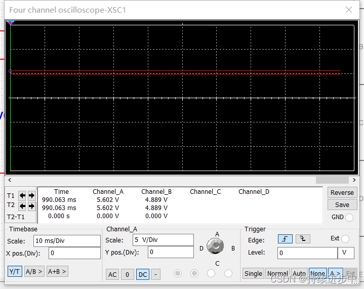
From the simulation results, it can be seen that the voltage stabilizing diode in this circuit stabilizes the voltage at 5.602V, The final output voltage of the circuit is 4.889V(5.602V - U B E U_{BE} UBE, Silicon tube 0.6V~0.7V), And the output voltage waveform is stable , The function of the circuit is basically realized .
2. Analysis of voltage stabilization principle
The following is about power supply changes and load changes , The output voltage adjustment process of triode series linear voltage stabilizing circuit is analyzed in detail .
1) Constant load , Input voltage U i n U_{in} Uin Reduce
When the load does not change , Input voltage U i n U_{in} Uin Less hours , Output voltage U o u t U_{out} Uout There is a downward trend . Due to the existence of Zener diode , The base voltage of the triode remains unchanged . here , The base - Emitter voltage U B E U_{BE} UBE increase . from Input characteristic curve You know , i B i_B iB With U B E U_{BE} UBE To increase with . Triode emitter junction forward bias , Collector reverse bias , be in Zoom in , Yes Δ i C = β Δ i B Δi_C = βΔi_B ΔiC=βΔiB, namely i C i_C iC increase . And because the circuit is a triode series voltage stabilizing circuit , The loop current is the same , U o u t = i C ∗ R l o a d U_{out} = i_C*R_{load} Uout=iC∗Rload, U o u t U_{out} Uout increase .
2) Constant load , Input voltage U i n U_{in} Uin increase
When the load does not change , Input voltage U i n U_{in} Uin increases , Output voltage U o u t U_{out} Uout There is an increasing trend . Due to the existence of Zener diode , The base voltage of the triode remains unchanged . here , The base - Emitter voltage U B E U_{BE} UBE Reduce . from Input characteristic curve You know , i B i_B iB With U B E U_{BE} UBE To reduce by . Triode emitter junction forward bias , Collector reverse bias , be in Zoom in , Yes Δ i C = β Δ i B Δi_C = βΔi_B ΔiC=βΔiB, namely i C i_C iC Reduce . And because the circuit is a triode series voltage stabilizing circuit , The loop current is the same , U o u t = i C ∗ R l o a d U_{out} = i_C*R_{load} Uout=iC∗Rload, U o u t U_{out} Uout Reduce .
3) Input voltage U i n U_{in} Uin unchanged , Load reduction
Input voltage U i n U_{in} Uin unchanged , When the load is reduced , Output voltage U o u t U_{out} Uout There is a downward trend . Due to the existence of Zener diode , The base voltage of the triode remains unchanged . here , The base - Emitter voltage U B E U_{BE} UBE increase . from Input characteristic curve You know , i B i_B iB With U B E U_{BE} UBE To increase with . Triode emitter junction forward bias , Collector reverse bias , be in Zoom in , Yes Δ i C = β Δ i B Δi_C = βΔi_B ΔiC=βΔiB, namely i C i_C iC increase . And because the circuit is a triode series voltage stabilizing circuit , The loop current is the same , U o u t = i C ∗ R l o a d U_{out} = i_C*R_{load} Uout=iC∗Rload, U o u t U_{out} Uout increase .
4) Input voltage U i n U_{in} Uin unchanged , Increased load
When the input voltage U i n U_{in} Uin unchanged , When the load increases , Output voltage U o u t U_{out} Uout There is an increasing trend . Due to the existence of Zener diode , The base voltage of the triode remains unchanged . here , The base - Emitter voltage U B E U_{BE} UBE Reduce . from Input characteristic curve You know , i B i_B iB With U B E U_{BE} UBE To reduce by . Triode emitter junction forward bias , Collector reverse bias , be in Zoom in , Yes Δ i C = β Δ i B Δi_C = βΔi_B ΔiC=βΔiB, namely i C i_C iC Reduce . And because the circuit is a triode series voltage stabilizing circuit , The loop current is the same , U o u t = i C ∗ R l o a d U_{out} = i_C*R_{load} Uout=iC∗Rload, U o u t U_{out} Uout Reduce .
summary
1) This paper introduces the characteristics of triode Input / Output characteristic curve ;
2) be based on Multisim A series linear voltage stabilizing circuit of triode is built ;
3) The design of triode series linear voltage stabilizing circuit is described in detail Output voltage adjustment process ;
The above is the whole content of this article , I hope this paper can be helpful for you to understand and use the triode series linear voltage stabilizing circuit .
Of course , If there is any mistake or imprecision in the content of this article , Please also point out in time , thank you !
Reference resources
Triode series voltage stabilizing circuit - regulated power supply - Electronic enthusiast network ;
Triode regulated linear power supply - CSDN Blog ;
Diagram of characteristic curve of triode ;
边栏推荐
猜你喜欢

Jetson Xavier NX source code compilation and installation ROS melody experience (failed)

(数电)各种触发器汇总——FPGA八股文(1)

Quanzhi t507 removes the IO expansion chip and retains the expansion pin function

如何把一个“平台” 塞进一个小盒子里?(下)|技术实现篇

Output PWM square wave with ls1028a development board
![[mindspore] [Lite end-to-side training reasoning] mindspore lit runs the lenet training example code according to the instructions and reports an error](/img/8c/db78bb0bcb75b7457c5e5f5c6cfd2a.jpg)
[mindspore] [Lite end-to-side training reasoning] mindspore lit runs the lenet training example code according to the instructions and reports an error
FPGA网口实现与详解(2)

FPGA刷题P1:4选1多路选择器、异步复位的串联T触发器、奇偶校验、移位拼接乘法

The end result of printf - where is the data printed

Mindspore dependent library not found
随机推荐
Intelligent gateway based on Ruixin micro 3568 core board
用LS1028A开发板输出PWM方波
i.MX8MP开发板移植USBWIFI RTL8192EU驱动
Allegro添加Drill Legend时不能显示Drill Legend信息之问题
1人天搞定9人天的日志接入开发——基于指令集物联网操作系统的项目开发实践
FreeRTOS线程安全、中断安全的printf实现方式
代码审计之若依系统
单电源运放和双电源运放及其供电方式选择与转换的注意事项
Mysql45 talking about reading notes in simple terms index (5)
SSH协议中隧道与代理的用法详解
How to test the availability and stability of EIM bus
瑞芯微RK3568开发板深度评测
RTOS——桌面mini网络时钟
Retinaface parsing
stm32f4 PWM捕获 (上升沿/下降沿/高低电平时间)详解(含代码)
G2L系列 核心板 -RZ/G2L 處理器簡介|框架圖|功耗|原理圖及硬件設計指南
Interpretation of text compression aided transformer encoding
i. Mx8mp development board porting USBWiFi rtl8192eu driver
提升开发效率的 Chrome 开发者工具快捷键参考
FPGA刷题P2:多功能数据处理器、求两个数的差值、使用generate...for语句简化代码、使用子模块实现三输入数的大小比较、使用函数实现数据大小端转化