当前位置:网站首页>Peripherals: I2C communication details
Peripherals: I2C communication details
2022-07-21 07:14:00 【Luxi Feixi】
What is? I2C signal communication
I2C The bus is made up of Philips The company developed a simple 、 Two way two wire synchronous serial bus . It only needs two wires to transmit information between devices connected to the bus .
The main device is used to start the bus to transmit data , And generate a clock to open the transmission device , In this case, any addressable device is considered as a slave device . Master and slave on the bus 、 The relationship between sending and receiving is not constant , And it depends on the direction of data transmission . If the host wants to send data to the slave , Then the master first addresses the slave , And then actively send data to the slave device , Finally, the data transmission is terminated by the host ; If the host wants to receive data from the slave device , First, the slave is addressed by the master . Then the host receives the data sent from the device , Finally, the receiving process is terminated by the host . under these circumstances . The host is responsible for generating the timing clock and terminating the data transmission .I2C Bus _ Baidu Encyclopedia
Physical interface :SCL + SDA
(1)SCL(serial clock): Clock line , transmission CLK The signal , It's usually I2C The master device provides a channel for the slave device to clock .
(2)SDA(serial data): cable , The communication data is transmitted through SDA Line transmissionCommunication characteristics : Serial 、 Sync 、 Non differential 、 Low speed rate
(1)I2C It belongs to serial communication , All data is in bits SDA Online serial transmission .
(2) Synchronous communication means that both sides of communication work under the same clock , It's usually communication A The square passes through a CLK Signal line transmission A Give your own clock B,B Working in A Under the transmission clock . So the salient feature of synchronous communication is : There is... In the communication line CLK
(3) Non differential . because I2C The communication rate is not high , And the two sides of communication are very close , So use level signal communication .
(4) Low speed rate .I2C Usually used on the same board 2 individual IC Communication between , And the amount of data used for transmission is small , So its communication rate is very low ( Usually hundreds of KHz, Different I2C The communication rate of the chip may be different , When programming, it depends on what is allowed by the equipment you use I2C Maximum communication rate , Don't exceed this rate )Outstanding features 1: Main equipment + Slave device
(1)I2C When communicating , The status of both sides of the communication is unequal , It is divided into master equipment and slave equipment . The communication is initiated by the master device , Dominated by the main equipment , The slave device just follows I2C The protocol passively accepts the communication of the master device , And timely response .
(2) Who is the main device 、 Who is the slave device is decided by both sides of the communication (I2C The agreement does not provide ), Generally speaking, a chip can only be the main device 、 It can also be used as a slave device 、 It can also be both a master device and a slave device ( software configuration ).Outstanding features 2: Multiple devices can be hung on one bus ( Slave device address )
(1)I2C Communication can be one-to-one (1 Master device pairs 1 Slave devices ), Or one to many (1 Master device vs. slave device ).
(2) The master device is responsible for scheduling the bus , Decide which slave device to communicate with at a certain time . Be careful : At the same time ,I2C Can only transmit the communication information of a pair of devices on the bus , Therefore, only one slave device can communicate with the master device at the same time , Other slave devices are “ hibernation ” state , Don't come out and make trouble , Otherwise, the communication will be disordered .
(3) every last I2C Slave devices have one in communication I2C Slave device address , This device address is an inherent attribute of the slave device , Then, when communicating, the master device needs to know the address of the slave device it will communicate with , Then in the communication, the address is used to identify whether it is the slave device you are looking for .( This address is unique on a circuit board , Not the only one in the world )Main uses :SoC Communication with peripheral devices ( A typical such as EEPROM、 Capacitive touch IC、 Various sensor etc. )
from I2C Learn communication timing IIC Bus details
What is timing ?
(1) sequential : Literally , Time sequence is time sequence , In fact, in communication, timing is the level change on the communication line in chronological order , And the significance of these changes to communication is called timing .I2C Bus idle state of 、 Start bit 、 End bit
(1)I2C There are... On the bus 1 A master device ,n(n>=1) Slave devices .I2C There are... On the bus 2 States ; Idle state ( All the slave devices are not communicating with the master device , At this time, the bus is idle ) And busy ( One of the slave devices is communicating with the master device , At this time, the bus is occupied by this pair , Other slave devices must rest ).
(2) The whole communication is divided into one cycle, one cycle , Two adjacent communication cycles are idle . Each communication cycle starts with a start bit , An end bit ends , In the middle is the communication data of this cycle .
(3) The start bit is not a point in time , The starting bit is a time period , The bus state changes during this period are :SCL The line maintains a high level , meanwhile SDA The line has a falling edge from high to low .
(4) Similar to the start bit , The end bit is also a time period . The bus state changes during this period are :SCL The line maintains a high level , meanwhile SDA The line has a rising edge from low to high .
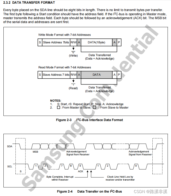
I2C Data transfer format ( Data bits &ACK)
(1) Each communication cycle is initiated and ended by the master device , The slave only responds passively to the master , I can't do anything by myself .
(2) The master device sends the first message in each communication cycle 8 Bit slave address ( Actually 8 There is only 7 Bit is the slave device address , also 1 Bit indicates whether to write or read from the master device ) To bus ( The master device is sent in the form of broadcast , As long as all the slave devices on the bus can actually receive this message ). Then each slave device on the bus can receive this address , After receiving the address, compare it with your own device address to see if it is equal . If it is equal, it means that the main equipment is talking to me this time , If you don't want to wait, this communication has nothing to do with me , Don't listen .
(3) After the sender sends a piece of data , The receiver needs to respond to a ACK. The response itself has only 1 individual bit position , Cannot carry valid information , It can only mean 2 What do you mean ( Or it means receiving data , That is, effective response ; Or it means that no data has been received , Invalid response )
(4) At a certain communication moment , Only one master device and one slave device can be active ( Take up the bus , That is, write to the bus ), The other is collecting ( Read from the bus ). If both master and slave devices try to write to the bus at some time, it's over , Communication is out of order .
Data transmission protocol on the bus
(1)I2C The basic data unit of communication is also in bytes , The valid data transmitted each time is 1 Bytes (8 position ).
(2) The starting bit and the following 8 individual clk The master device is sending ( This device controls the bus ), At this time, the slave device can only read the bus , Read the bus to know the information sent by the master device to the slave device ; And then to the 9 cycle , According to the agreement, the slave device needs to send ACK To main equipment , Therefore, the master device must release the bus at this time ( The master sets the bus to high level and then does not move , In fact, it is similar to the bus idle state ), At the same time, the slave device attempts to pull down the bus ACK. If pulling down the bus from the device fails , Or the slave device doesn't pull down the bus at all , The phenomenon seen by the master device is that the bus is on the 9 The cycle remains high , This is for the main equipment , It means I didn't receive ACK, The master device thinks that the message just sent to the slave device 8 Wrong byte ( Reception failed )

S5PV210 Of I2C controller
Both sides of communication are essentially working through timing , But the timing will be more complex, which is not conducive to SoC Software complete , So the solution is SoC The controller with built-in hardware generates the communication sequence . In this way, when writing software, we only need to write the configuration value to the register of the controller , The controller will generate appropriate timing to communicate with each other on the communication line .
Structure diagram
(1) The clock part , The source of the clock is PCLK_PSYS, After internal frequency division, we finally get I2C Controller CLK, In communication CLK Will pass SCL Line to slave .
(2)I2C Bus control logic ( The front desk representative is I2CCON、I2CSTAT These two registers ), Mainly responsible for generating I2C Communication timing . In actual programming, the start bit should be sent 、 Stop bit 、 receive ACK And so on through these two registers ( The circuit module represented behind ) Realized .
(3) shift register (shift register), The byte data to be sent in the code , Through the shift register, it becomes 1 Bit by bit, throw it to SDA Send online / receive . Students who have learned digital circuits should be familiar with shift registers .
(4) Address register + The comparator . Ben I2C The controller is used as a slave device .( I've never used , The theoretical analysis )Systems analysis I2C The clock of
(1)I2C Clock source comes from PCLK(PCLK_PSYS, be equal to 65MHz), After 2 Obtained after stage frequency division .
(2) The first stage of frequency division is I2CCON Of bit6, You can get an intermediate clock I2CCLK( be equal to PCLK/16 perhaps PCLK/512)
(3) The second stage of frequency division is to get the final I2C The clock that the controller works , With I2CCLK This intermediate clock is the source , The frequency division coefficient is [1,16]
(4) The final clock is 2 Clock after stage division , For example, one of the available settings is :65000KHz/512/4=31KHz1.12.3.3、 Main register I2CCON、I2CSTAT、I2CADD、I2CDS
I2CCON + I2CSTAT: It is mainly used to generate communication sequence and I2C Interface configuration .
I2CADD: Used to write your own slave address
I2CDS: send out / The received data is put here

X210 On board gsensor Introduce
Schematic view
(1)gsensor The power supply for is provided by PWMTOUT3 Pin control . When PWMTOUT3 Output low level gsensor No electricity, no work ; When the output is high gsensor To work .
(2)gsensor Of SDA and SCL The next thing is S5PV210 Of I2C port 0
(3) When programming in the future gsensor_init Function to initialize related GPIO. Corresponding GPIO Set to the correct mode and input / output values .Introduction to gravity acceleration sensor
(1) Used on mobile phones 、 Flat 、 Smart watches, etc , Used to feel the movement of people's hands , Obtain some directional information of motion and use it as input parameters to the system .
(2) It can be used to design the pedometer function of smart watches .
(3) Gravity acceleration sensor 、 Geomagnetic sensor 、 Gyroscope and other three sensors are combined , Are used to thank the speed of movement 、 Orientation and other information , So now the latest ones are 9 Shaft sensor , Is to combine the three , And use a certain algorithm to synthesize and draw a conclusion , The purpose is to be more accurate .
(4) Generally, the interfaces of sensors are 2 Kind of : Analog interface and digital interface . Analog interface uses interface level change as output ( For example, the pressure sensor of analog interface , When the pressure is different, the output level is 0~3.3V Range change , Each voltage corresponds to a pressure .),SOC Need to use AD Interface to connect the sensor and analyze its output data AD transformation , Convert to digital voltage value , Then calibrate the digital voltage value to obtain the pressure value ; Digital interface was developed later , Digital interface sensor It is at the of the analog interface sensor On the basis of , Internal integration AD, direct ( Through a certain bus interface protocol , It's usually i2C) A parameter that outputs a numeric value , such SoC Initialize directly through the bus interface 、 Just read the parameters output by the sensor ( for example gsensor、 Capacitive touch screen IC).I2C The device address of the slave device
(1)KXTE9 Of I2C The address is fixed to 0b0001111(0x0f)
(2)I2C The slave address itself is 7 Bit , But in I2C Send in communication I2C What is actually sent from the device address is 8 position , this 8 Middle high 7 position (bit7-bit1) Corresponding I2C From the device's 7 Bit address , The lowest one (LSB) Deposit is R/W Information ( That is to say, the next data is written by the master device and read by the slave device ( Corresponding 0), The master device reads and the slave device writes ( Corresponding 1))
(3) Based on the above , about KXTE9 Come on , Main equipment (SoC) issue gsensor Information ,SAD Should be :0b00011110(0x1E)
If it is read by the master device gsensor Information ,SAD Should be :0b00011111(0x1F)I2C The communication rate of the slave device
(1)I2C The protocol itself is a low-speed Protocol , The communication rate should not be too high .
(2) In fact, the master and slave devices of communication have the highest communication rate limit ( Parameters belonging to each chip itself ), How to determine the final communication rate during actual programming ? As long as it is less than two .
(3) Generally speaking, it can only be used as a slave device sensor The chip itself i2c The communication rate is low , image KXTE9 The highest support 400KHz The frequency of .
I2C Communication flow of bus
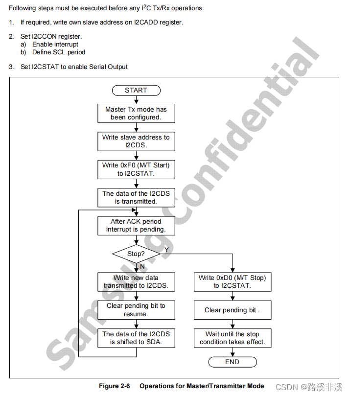
S5PV210 Main sending flow chart
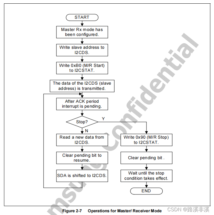
S5PV210 Main receiving flow chart
gsensor Write register flowchart
gsensor Read register flowchart
I2C Communication code analysis
I2C Controller initialization :s3c24xx_i2c_init
(1) Initialize what you do : initialization GPIO, Set up IRQEN and ACKEN, initialization I2C The clock
I2C The controller starts reading and writing in main mode :s3c24xx_i2c_message_startI2C The main mode of the controller ends one reading and writing :s3c24xx_i2c_stop
I2C Communication code analysis 2
Frame analysis : Our ultimate goal is to read and write gsensor The internal register of the chip to get some information . In order to achieve this goal , We need to be able to read and write gsensor The register of , according to gsensor We need to read and write according to certain operating procedures gsensor The internal register of , This is a level ( Let's call it the transport layer 、 Protocol layer 、 application layer ); We should read and write registers according to the operation flow , You need to think about I2C Interface protocol ( This is the so-called physical layer , The essence is those timing ). At this time, the host SoC With or without controller , When there is a controller, consider the register of the controller , When there is no controller, you should simulate the timing with your own software .
The code of the protocol layer mainly depends on gsensor chip ; The physical layer code mainly depends on the host SoC.
gsensor Write register :gsensor_i2c_write_reg
gsensor Read register :gsensor_i2c_read_reg
gsensor Programming :gsensor_initial etc.
边栏推荐
- 【电脑小工具推荐】久坐提醒
- PostgreSQL是什么?StackOverflow上开发者最爱和最想要的关系型数据库
- The ability to detect movement in vivo and build a safe and reliable payment level "face brushing" experience
- [technical dry goods] driver development and abnormal analysis of industrial touch screen (serial)
- 【C语言】计算器实现
- Analyzing the internal mechanism and breakthrough path of "Web3 paradox"
- 外设篇:SD卡等外存设备
- 自定义类型:结构体,枚举,联合
- RKE vs. RKE2:对比两种 Kubernetes 发行版
- Simulate the readline() function of BufferedReader with reader
猜你喜欢


![[shutter -- top navigation bar] basic use of tabbarview](/img/01/c588f75313580063cf32cc01677600.jpg)
随机推荐
获取系统信息
Dynamic memory management (malloc, free, calloc, realloc, flexible array)
Video analysis streameye studio
C陷阱和缺陷 第0章 导读
【Flutter -- 基础组件】图片组件 Image & Icon
Start to build a three node Eureka cluster
DAO的精简化治理的委托机制
动作活体检测能力,构建安全可靠的支付级“刷脸”体验
基于NLua实现使用lua脚本中多线程执行方法
Possibilities and limitations of defi in the metauniverse
Postgresql中函数详解看一篇就够了——常用函数以及使用方法
How to download video files
DeiT:注意力也能蒸馏
C和指针 第1章 词法“陷阱” 1.4 整型常量
ARM 如果通过笔记本机上外网?
Data quality construction of data warehouse
KubeSphere 3.3.0 离线安装教程
Alibaba cloud load balancing experiment July 11, 2022
(note) feature fusion method in neural network (add/connect)
数据库表设计规范汇总