当前位置:网站首页>[advanced semiconductor process technology series] SOI Technology (Part 2)
[advanced semiconductor process technology series] SOI Technology (Part 2)
2022-07-21 23:27:00 【Da Biao loves work】
SOI Technical introduction 、SIMOX technology 、BESOI technology 、Smart-Cut Technical details :《【 Semiconductor advanced process technology series 】SOI technology ( On )》
PD-SOI technology 、 Warping effect 、 Parasitic bipolar transistor effect 、 Self heating effect 、 Body contact see :《【 Semiconductor advanced process technology series 】SOI technology ( in )》
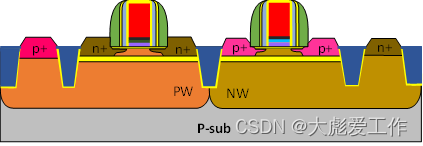
FD-SOI Process technology
PD-SOI There is not only floating body effect , And with SOI The process technology has developed to the nanometer level ,PD-SOI The short channel effect of devices is becoming more and more serious , And for FD-SOI device , When the device works in the saturation region , Silicon thin films are completely depleted , The potential barrier between the source and the body is very small , Holes are easily compounded in the source region without accumulation , So the floating body effect is right FD-SOI The influence of devices is very small , in addition FD-SOI The thin junction depth of the source and drain of the device can reduce the width of the transverse diffusion of the source and drain depletion layer , So as to effectively inhibit the short channel effect ,FD-SOI Devices are widely used in nanoscale processes .
FD-SOI In addition to improving the floating body effect and short channel effect , It also has many other advantages , Including unique back offset capability , Low supply voltage ( The minimum supply voltage is close to the threshold voltage , You can achieve 0.4V), Low leakage current , Low parasitic capacitance , Strong ability to resist radiation , Strong transistor matching characteristics and high device working speed . These advantages make FD-SOI Used in smart phone processors 、 Autopilot chip 、 Internet of things chips 、 Applications such as communication transceivers and automotive electronics .
FD-SOI Technological process
FD-SOI Technology and MOSFET Planar process is compatible ,FD-SOI The first stage of the process technology adopts the first grid HKMG And strained silicon technology , The latter part is still the copper process of Damascus structure .
1.SOI Substrate preparation .

2. Deposit SiO2 and Si3N4, And formed by photolithography and etching STI;

3. adopt HDP CVD Deposit SiO2, And then through CMP Flatten ;

4. Remove SiO2 and Si3N4, And formed by photolithography and ion implantation NW and PW;

5. By photolithography and etching , Remove NW and PW Contact oxide buried layer ;

6. By selective epitaxial growth PW and NW Contact area of ;

7. Deposit SiON,HfSiON,La2O3 and TiN Metal cladding ;

8. Remove by photolithography and etching PMOS The gate dielectric layer of the region ;

9. Deposit SiON,HfSiON,Al2O3 and TiN Metal cladding , And remove by photolithography and etching NMOS The gate dielectric layer of regional secondary deposition ;

10. Depositing polysilicon gate .

11. adopt LPCVD Deposit SiO2 and SiON Hard mask layer ;

12. Hard mask plate layer is formed by photolithography and etching ;

13. The gate is formed by etching ;

14. Deposit SiO2 and Si3N4, And the isolation side wall is formed by etching ;

15. Formed by photolithography and ion implantation LDD structure ;

16. Deposit SiO2,Si3N4 and SiO2, And the second isolation side wall is formed by etching ;

17. utilize LPCVD Deposit a layer SiO2 Oxide layer , As SiGe Barrier layer for epitaxial growth ;

18. By photolithography and etching , Remove NMOS Regional SiO2 Oxide layer . Then etch the silicon substrate by selective etch back technology , stay n The active area forms grooves ;

19. Strained silicon material is formed by epitaxial growth SiC Of n Type active area ;

20. utilize LPCVD Deposit a layer SiO2 Oxide layer , As SiGe Barrier layer for epitaxial growth ;

21. By photolithography and etching , Remove PMOS Regional SiO2 Oxide layer . Then etch the silicon substrate by selective etch back technology , stay p The active area forms grooves ;

22. Strained silicon material is formed by epitaxial growth SiGe Of p Type active area ;
23. formation Salicide.

FD-SOI The process technology is to use epitaxial growth technology to bulge the source and drain active regions , Source and drain doping at the same time , because FD-SOI The active region of is very thin , The source and drain active regions are raised by epitaxial growth technology , The thickness and surface area of the active region can be increased , Thus forming a thicker Salicide, Reduce the contact resistance of source and drain . stay PMOS Source and drain active region epitaxial growth SiGe Strain material and in NMOS Source and drain epitaxial growth SiC The strained material can produce stress in the device channel , Increase the carrier speed , Finally improve FD-SOI The speed of the device .


Related content
《【 Semiconductor advanced process technology series 】 Strained silicon technology 》
《【 Semiconductor advanced process technology series 】HKMG Process technology ( On )》
《【 Semiconductor advanced process technology series 】HKMG Process technology ( Next )》
《【 Semiconductor advanced process technology series 】SOI technology ( On )》
《【 Semiconductor advanced process technology series 】SOI technology ( in )》
边栏推荐
- Hcip second day comprehensive experiment
- Understanding of timer bidirectional break inputs based on stm32h7x3 series
- Unity uses BVH to drive bone movements
- Summary of common methods of string
- HCIP day1
- Real estate giant, data integration construction project plan (take it away, no thanks)
- [contents, methods, tools and results of information collection]
- HCIP:ospf第一节
- TCP three handshakes and four disconnects
- MySQL delete a large number of data tables are locked, and the thread is in the killed state after killing the thread. The problem is solved
猜你喜欢

Static routing extension

2021 MCU WiFi competition new pattern, domestic MCU WiFi chip inventory, appendix 2020/2021 MCU WiFi ranking

Rip routing information protocol

OSPF working process and its simple experiment

C # from entry to mastery (I)

Hcip mGRE comprehensive experiment

Single arm routing configuration

The path problem of downloading, reading and storing JSON files by hololens (personal hololens2 advanced development summary I)

Software development of AGV mode API call

All equipment, accessible throughout the network
随机推荐
Unity lock the arc motion of the camera around the locked target
MGRE实验
Analyze examples and immersively master important concepts of matter
Silabs matter full stack solution, appendix high quality matter training materials
HCIP第二天RIP
关于char str[20]=““ 和 char str[20]=“ “
Data visualization application installation and deployment | common problems tutorial using datart installation package and source code deployment
raptor 可视化工具
STM32 series timer complementary output details
HCIA rip experiment
探索式软件测试
Understand the composition and working principle of cache
JS基础知识
The image after the RGB and a channels are separated from the atlas, and the original image is exported after the RGBA channel is merged
Unity based hololens2 and server for JSON, model and video streaming practice (personal hololens2 advanced development summary)
Mongodb complex query instance (nested multiple arrays and regular expressions)
ms17_010 入侵Win7
Summary of common methods of string
Reading and writing properties file
Experiment 2 - white box testing - software quality assurance and testing